Two-photon high-precision three-dimensional laser direct writing and three-dimensional photon bridging
Release Time:
2024-11-04
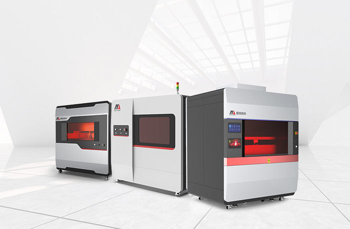
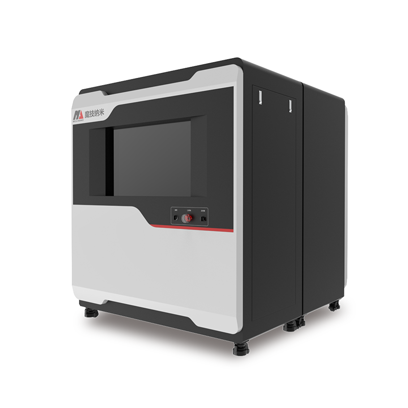
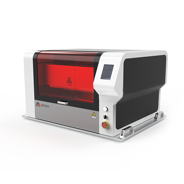
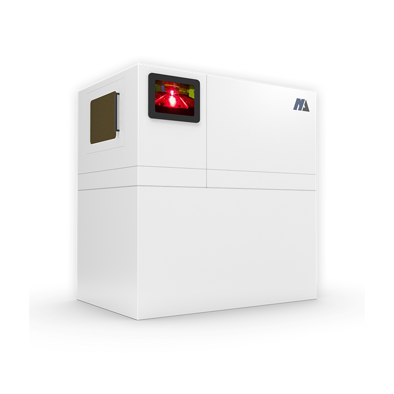
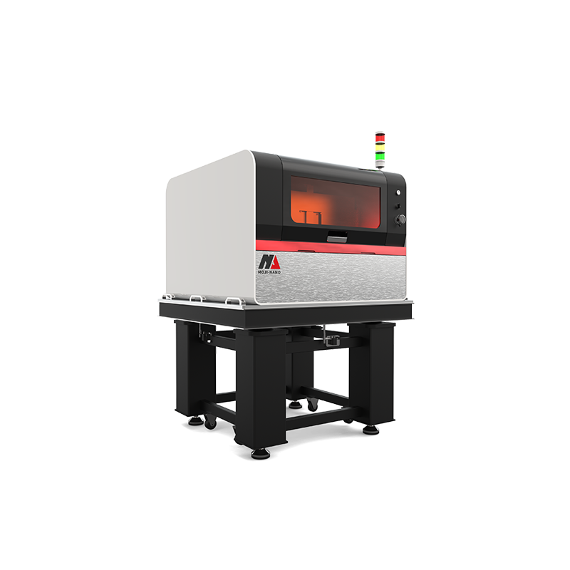
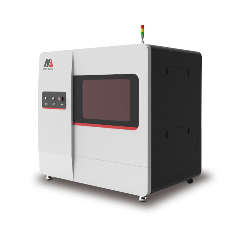
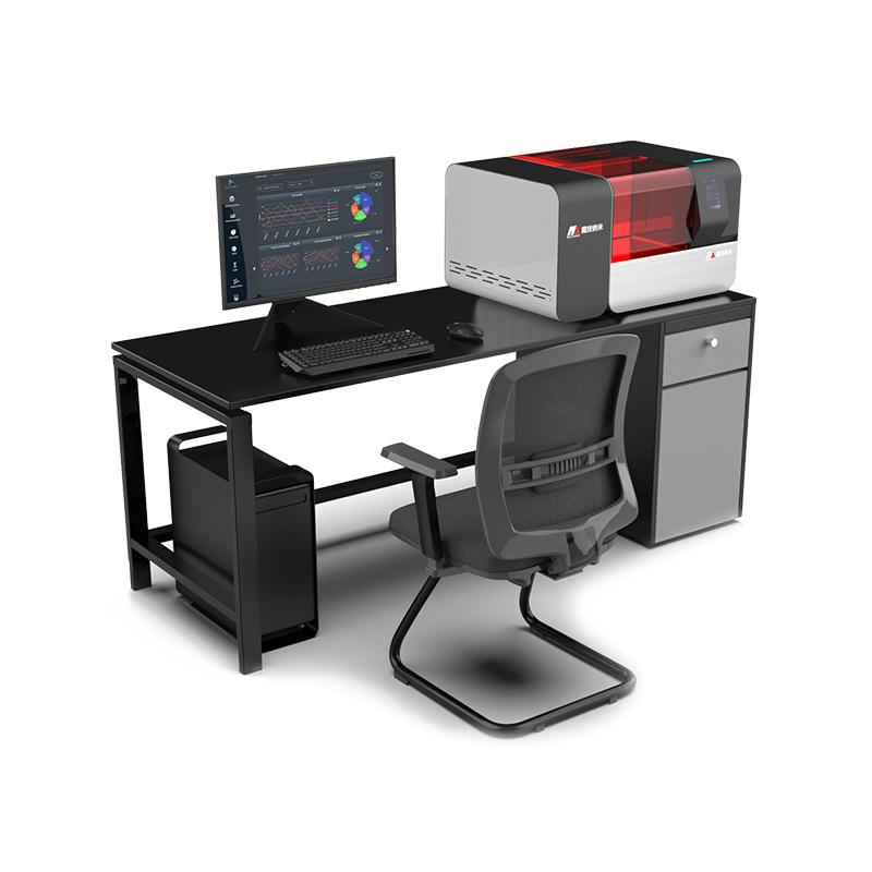
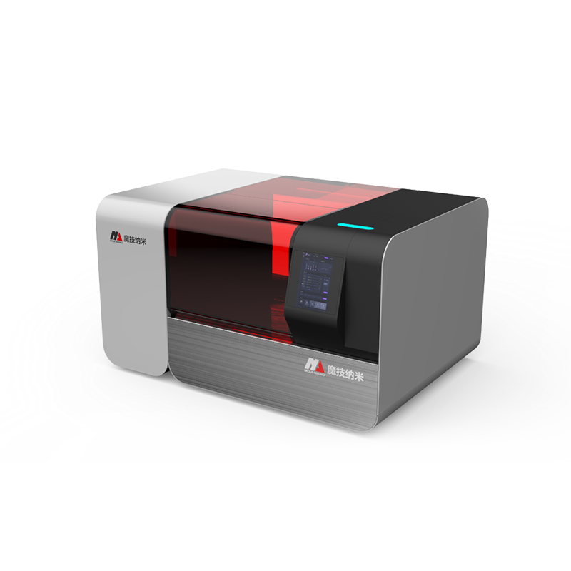
Moji- Nano is the manufacturer of domestic commercial nano-scale three-dimensional laser direct writing manufacturing system, using the world's advanced laser infinite field of view point-by-point direct writing technology.
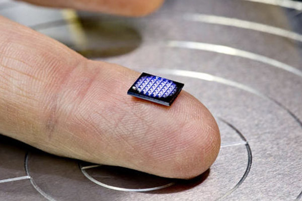
Silicon optical chips not only have the basis of mature technology, high integration, and low price of microelectronics, but also have the advantages of high bandwidth, ultra-fast rate, anti-interference, and low power consumption of optoelectronics. They have been touted by many technology companies at home and abroad. It has become a hot spot for semiconductor and communications companies. It will play an important role in future optical storage, optical display, optical interconnection, optical computing, as well as future medical and health care, aerospace, and national defense.Whether from the perspective of getting rid of the difficulties of the domestic industry or catching up with the global pace, it is urgent to develop new methods and technologies for independent and controllable “China Optoelectronics chips”.China's silicon optical chips are not perfect in terms of design, preparation, packaging, testing, etc. Most of the silicon optical chips require foreign OEM, coupling between silicon optical devices, and high-density integration and other key technical problems need to be solved.Three-dimensional laser direct writing with high speed, cross-scale, and nanoscale high precision is a key technology for preparing new photonic materials and devices and improving their performance, which has an important impact on the development of the field of silicon optical chip integration.Although micro-nano 3D printing technology based on femtosecond laser two-photon or multi-photon polymerization has high nanoscale three-dimensional processing capabilities, it also has the disadvantage of low processing efficiency, which seriously limits the application of such technologies in large-scale integrated silicon optical chip manufacturing.
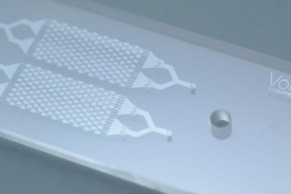
Using nano-scale three-dimensional laser direct writing technology, a three-dimensional optical waveguide structure is processed on an optoelectronics chip, which is used to realize the coupling and interconnection between different optical chips, chips and optical fibers, so as to effectively connect various photonic integration platforms and simplify the assembly process of advanced optical multi-order modules, which can be used as an additional three-dimensional photonic integration technology.At the same time, it combines light field regulation technology to realize multifunctional parallel three-dimensional nano-processing, and uses the multi-parameter modulation of the light field to construct a multi-dimensional, high-precision, high-speed, and cross-scale dynamic three-dimensional integrated coupling for silicon optical chips. It solves the key problems of low coupling efficiency, high loss, and high cost in the coupling and integration applications of high-precision three-dimensional nano-manufacturing between silicon optical chips, breaks through a number of technical bottlenecks, and lays the foundation for the subsequent preparation of silicon optical chip integrated devices with more complex structures and more complete functions, and promotes nanoscale three-dimensional laser direct writing related technologies to the silicon optical chip industry application field.
News Recommendation


