➤ Hybrid Optoelectronic Chip - Network Integration
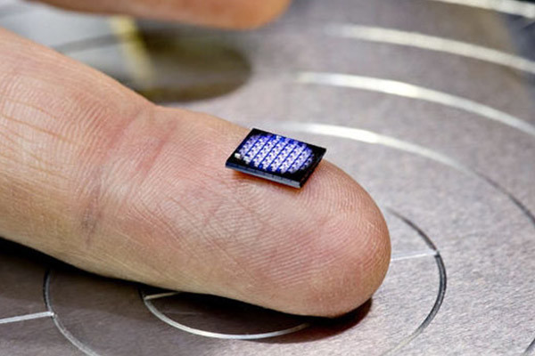
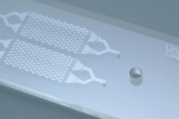
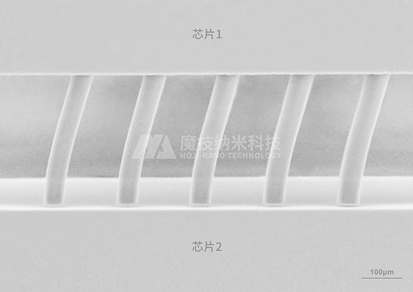
With the evolution of Moore's Law and the continuous demand for the improvement of chip technology from applications including 5G, the Internet of Things, automotive electronics and high-performance computing, more advanced packaging technologies are also being continuously promoted. Compared with traditional packaging, advanced packaging technologies are more efficient. Chips are evolving towards being smaller and thinner, with lower amortized costs and better cost performance. In the integration process of chips, especially optical chips, it is necessary to bridge different chips. By utilizing nano three-dimensional manufacturing, fixed-point linking can be achieved between different chips without the need for a second-step operation. It is simple to fabricate, with high precision and low transmission loss.
The three-dimensional micro-nano direct writing lithography technology of MOJI-NANO technology can achieve highly free three-dimensional connections, greatly reducing the connection loss between chips and the packaging cost, and realizing the freedom of silicon photonics chip packaging.
Technical advantages:
● Achieve low-loss connections between silicon optoelectronic chip networks;
● Realize the automation of silicon photonics chip network connections and improve connection efficiency;
● Achieve micron-scale connections and highly integrated connections;
● Achieve free connections between silicon-based photonic chips in three-dimensional space.


➤ Applications of Optical Fibers
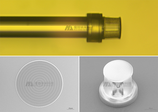
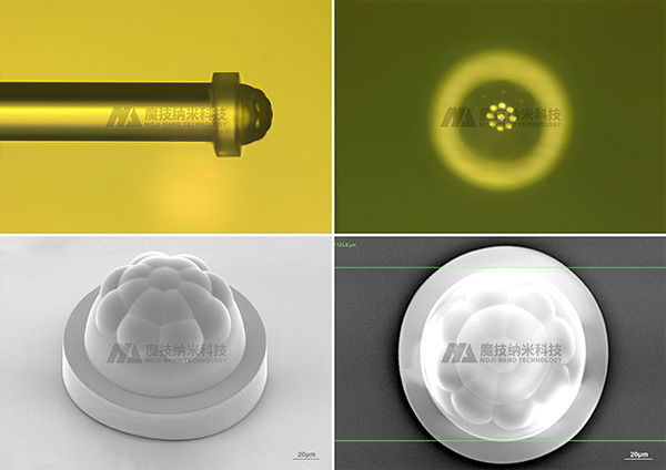


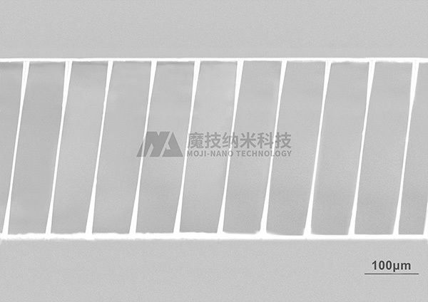
By leveraging the principle of multiphoton polymerization, nanometer-level precise alignment can be realized. Nanometer-level 3D processing can be performed on the fiber core, the surface as well as the interior of optical chips. The distribution and arrangement of materials can be precisely controlled and optimized to customize and optimize optical properties and transmission characteristics, create complex optical components, and achieve a high-precision structural layout. Thereby, high-throughput, precise and rapid production can be achieved to meet the requirements of different applications of optical fibers.
➤ High-performance sensors
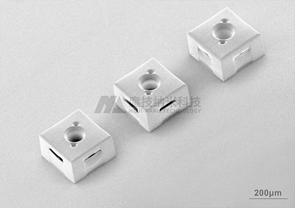
Nano 3D manufacturing is replacing electron beam lithography technology to produce plasmonic nano-antenna arrays for use in chemical and biological sensors. The manufacturing process is more reliable, faster, simpler and of lower cost.


Address
No. 1 Rongchang Road, Huangbohai District, Yantai City, Shandong Province, China
Subscribe
Get the latest information from Moji Nano Technology
Scan WeChat QR Code to Contact Us
